Making a correction
Introduction
Pre-compensate designs to counteract fabrication effects. This example shows how to correct the same 500 nm target structure, automatically adjusting the layout so the fabricated result matches your target specifications.
Import the library:
Loading a device
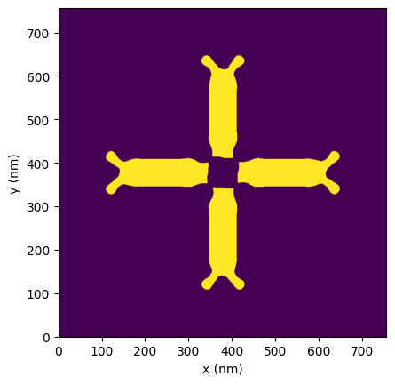
Create your target device - the structure you want to fabricate. The Device class represents photonic geometries in PreFab - load from GDS, images, or numpy arrays with binary pixel values (0 or 1).

Correcting a device
Run a correction using a specific fabrication model. Reach out if you'd like a model trained for your fabrication process.
Note
Initial prediction/correction may take longer due to server startup and model loading. Subsequent predictions should be quicker.
MODEL_NAME = "Generic_SOI"
correction = device.correct(model=pf.models[MODEL_NAME])
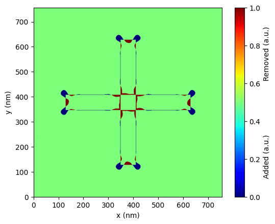
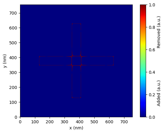
correction.plot(show_buffer=False)
The correction model pre-distorts the layout to compensate for fabrication effects - adding material where erosion is expected, removing it where dilation occurs.
Making a prediction of the correction
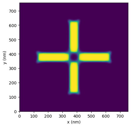
Verify the correction by predicting the fabrication outcome. The corrected design shows sharper corners and better-resolved features. The IoU score improves from 83% to 95% - meaning the fabricated device will match your target specifications far more closely.
outcome = correction.predict(model=pf.models[MODEL_NAME])
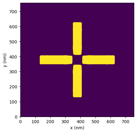
outcome_bin = outcome.binarize()
outcome.plot(show_buffer=False)
outcome_bin.plot(show_buffer=False)
outcome_bin.plot_compare(ref_device=device, show_buffer=False)
While perfect restoration isn't always achievable due to physical constraints, correction consistently recovers significant performance. Stay updated with the latest models as we continue improving accuracy.